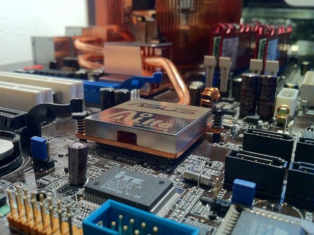
The Printed Circuit Board or the printed wiring board becomes a Printed Circuit Boards Assembly (PCBA) when the electronic components are placed on it in their designated places. The first step of PCB designing is the etching out of the copper tracks on the Printed Circuit Boards which involves the ironing of the designed print of the integrated circuit onto the board and then treating it with chemicals for the tracing of the tracks.

Circuit board components are placed on the surface of the PCB in order to get the required device that we need. The placing of the component on the surface of PCB is done with the help of special surface mount technology (SMT) equipment which allows for high efficiency and neatness to be achieved.
A list and detail of some of those components are given below:
- Solder Paste Application Machines
The first stage of the Printed Circuit Boards assembly is the application of solder paste on the surface of the PCB. The solder paste is applied only to certain places of the board i.e. where components are to be placed as per the design of the integrated circuit board.
- Reflow Soldering Machine
The third step in the assembly process of printed circuit boards is the reflow soldering process in which the soldering paste is heated to be melted and solidified again so as to affix to components to their designated places.
- Cold Pressing M/C
Cold Pressing Machine is employed in order to engage the copper layer with the surface of the printed circuit board. It is also used to strengthen the solder paste applied during the assembly process in order to keep the components firmly in their place.
- Orbotech 1450 AOI with Repair Station
The standard technique of inspection of the PCB assembly is the automatic optical inspection which is done with the help of AOI machine.
- Placing of the Components (SMT)
After the application of solder paste to the surface of the PCB has been completed, the board moves to the pick and place machine where the components are placed by the machine to their designated places.
- X-Ray Inspection
The less common method of inspection is the x-ray inspection and used only for layered PCBs. The x-ray inspection allows seeing the inner layers of the PCBs and any problem which may be associated with them.
A list of above-given technology equipment are used by industry for the smooth execution of Printed Circuit Board Assembly process.

